Menu:
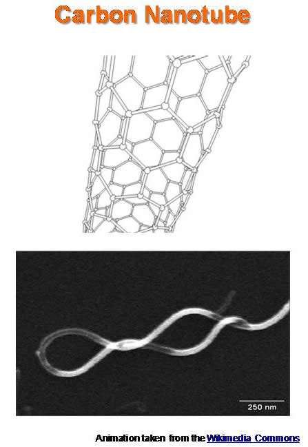
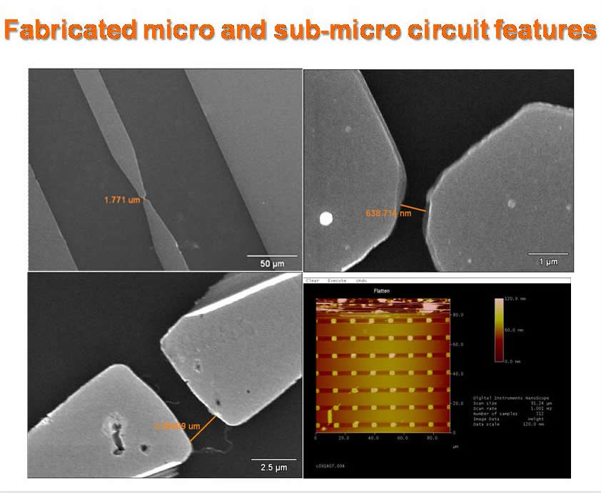
Carbon nanotubes (CNT), since their discovery in 1991, have intrigued so many interests in extensive research fields attributed to their unique electrical, mechanical and thermal conduction properties. A great variety of applications have been proposed and demonstrated, such as CNT FET, CNT field emission display, and CNT super capacitor etc. In microwave and THz frequency range, many applications have been suggested as well, including CNT interconnects, CNT antennas etc. To shed the light for potential applications in microwave and THz frequency range, novel high-frequency characterization methods need to be developed to characterize carbon nanotubes. At the same time, the current available software for numerical EM simulation, such as ADS momentum and HFSS, can be well utilized to serve various purposes for CNT circuit design. Our research effort has been mainly dedicated in the following fields: microwave and THz characterization of ensemble of CNTs (i.e. CNT film, CNT paper) and individual CNT, CNT growth with patterned catalyst, and EM simulation for potential CNT applications. Various fabrication and imaging facility including NPGS system (for electron beam lithography), mask aligner, field-emission SEM, TEM, and AFM are conveniently accessible on UA campus. An in-house CNT growth equipment has also been set up running. |
|||
 |
 |
||
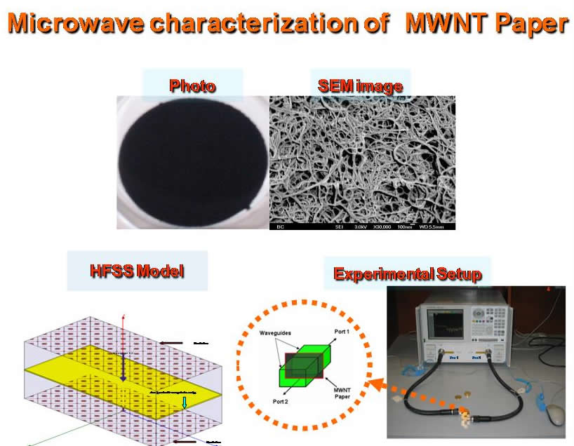
Microwave characterization of multi-walled carbon nanotube (MWNT) paper |
|||
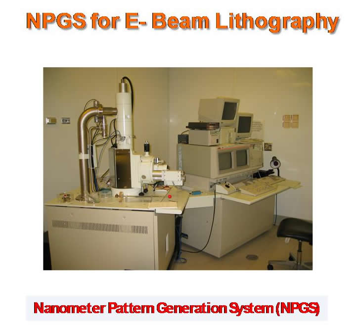
High frequency characterization of individual CNT Fabrication facilities: http://usif.arizona.edu/about.html http://www.chem.arizona.edu/facilities |
|||
  |
|||
| E-beam lithography equipment |
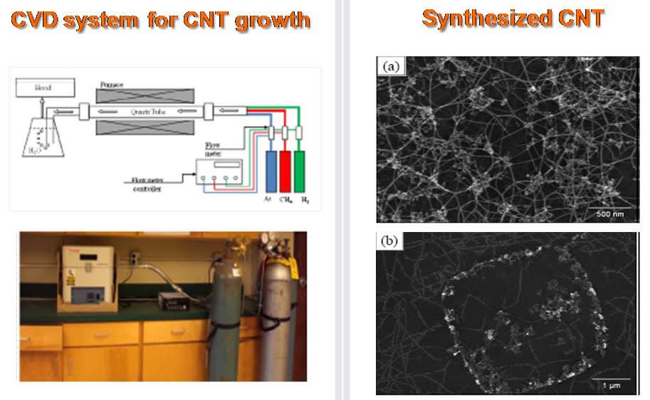
CNT growth with patterned catalyst |
||

ECE| UArizona |
Links
Running on mwca@ece3 - Contact :wzr@ece.arizona.edu